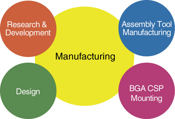
Technology
Introduce Technology For Keywords
-
Advanced design technologies
Superior pattern design by our certified (JPCA level one and two Certified Printed wiring Designers) design engineers.
-
Short delivery shift
Design support, using two shifts, 24 hours a day, 365 days a year.
-
Impedance control wiring
With simulations and comunication with the manufacturing site, we are able to design patterns with emphasis on impedance control.
-
DFM verification
With almost 300 design rules used in designing, we are able to detect problematic processes and improve prior to manufacture, thus cutting down the number of prototypes needed.
-
EMC design services
Using 39 chapters of Electronic rules regarding EMC, SI, PI, etc, we are able to instruct EMC design effectively.
-
Silicone free
Type zero (0) contains no Siloxane.
-
Environmental conservation / cost-reduction
Repairs to Magic resin (reforming), recycling of the carrier base material, and shaping of the resin to customer demands.
-
Response to a high-speed signal
With our Lamination technology that creates even thickness on each layer, and our conductor processing, we are able to create a highly stable impedance controlled product.
-
High density
High density boards utilizing Laser drilled vias, Fill-plating, stacked vias and build-up lamination technology.
-
Thinner boards -1
Ultra-thin multi-layered build-up boards utilizing ultra-thin cores, or coreless boards.
-
Thinner boards -2
By combining flex boards and build-up technology, our Flex rigid boards require no connector boxes, thus saving space, and with laser drilling, we can achieve thinner, smaller boards.
-
Downsizing -1
Achieve downsizing with the latest laser drilled via shaping, and improved fine-pitch wiring density
-
Downsizing -2
By combining flex boards and build-up technology, our Flex rigid boards require no connector boxes, thus saving space, and with laser drilling, we can achieve thinner, smaller boards.
-
Connection reliability
By utilizing the board edges with half-through hole technology, we increase the area and adhesion of solder, thus providing better connectivity.
-
Conserving space
By utilizing component mountable cavities, we are able to lower the board's height and save space.
-
High durability and high reliability
Experienced in supplying boards requiring high durability and high reliability in our multi-layer through-hole boards for the automotive, medical, and industrial (robotics) industries.
-
Multi-pin densification
Using laser processing and semi-additive patterning, we can provide higher pin count with higher density.
-
Small quantity, large variety
We have solutions for your small quantity large variety issues.
-
Prototype short delivery
Capable of very short delivery times.
-
Mass production
Open to suggestions such as Overseas production or VE, VA that will increase competetiveness.
-
Security
We offer the service and support that only a trusted PCB maker can offer.